Silicon Wafers Micron For Solar Panel

Cross Sectional Device Structure Of Abc Silicon Wafer Solar Cell Download Scientific Diagram

Raytonsolar Silicon Solar Wafer Manufacturing Reduces Costs By 60 While Making Them 25 More Efficient Solar Particle Accelerator How To Remove

Float Zone Wafers 5 Facts You Need To Know Wafer World Inc Semiconductor Micron Technology Wafer

Monocrystalline Silicon An Overview Sciencedirect Topics
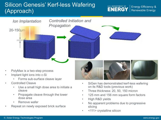
Sigen Targets Thin Silicon Wafers With Ion Implant Technology For Solar Pv Greentech Media

What Is The Manufacturing Principle Of Solar Cell Silicon Wafer Knowledge Ds New Energy

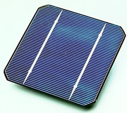
Origin has already produced commercial solar panels using a new silicon wafer called sliver technology at a facility in australia.
Silicon wafers micron for solar panel.

Stanford Creates Flexible High Efficiency Peel And Stick Solar Cells Extremetech

Gaas Wafer Advantages Of Gallium Arsenide Over Silicon

Solar Silicon Substrates For Research And Production

Pin On Solar Power

Manufacturers Look To Gain From Propriety Technologies In Pv Module In Solar Energy Market In 2020 Solar Energy Renewable Energy Resources Solar

Pin On New Home Decoration Design

Bill Nye The Science Guy Backs Revolutionary Solar Company Solar Companies Science Guy Solar

The Schematic Representation Of Monocrystalline Si Solar Cell Download Scientific Diagram

Chinese Chip Firm Fujian Jinhua Denies Stealing Ip From Micron Https Www Oann Com Chinese Chip Firm Fujian Jinhu Memory Chip Micron Technology Semiconductor

Http Www Electronicsandyou Com Blog Top Electronic Companies In Usa Html Electronics Companies Semiconductor Technology Micron Technology

Solar Wafer Solarfeeds Marketplace

Usa Semiconductor Companies Semiconductor Technology Micron Technology Semiconductor

6 034 Silicon Wafer Dallas Semiconductor Ds1775 I2c Thermometer And Ds2016 Sram Semiconductor Thermometer Wafer

Pin On Patio Lawn Garden

Pin By Aminul Hoque Chowdhury On Off Greed Energy Bangladesh Electronic Products Bluetooth Electronics

Sailing Drone Measures Oceans Autonomously For 12 Months

Crystalline Silicon Solar Cell An Overview Sciencedirect Topics

Solar Wafer Pricing
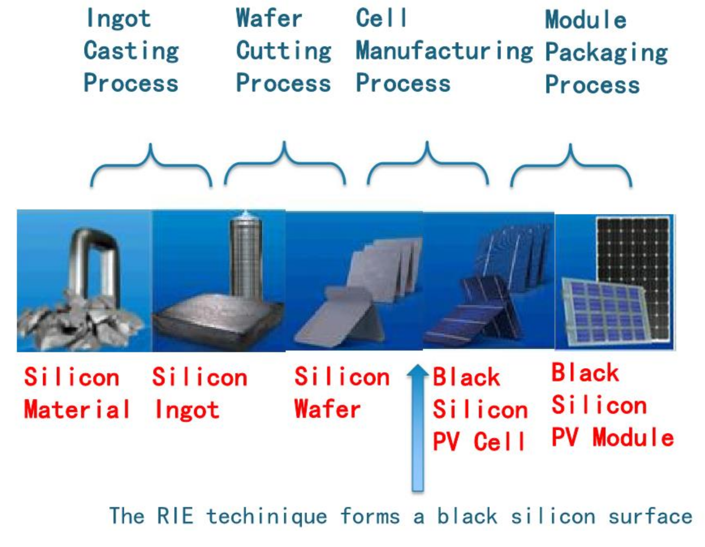
Crystals Free Full Text Research On Performance Improvement Of Photovoltaic Cells And Modules Based On Black Silicon Html

Silicon Wafer Supplier Turning Silicon Wafers Into Solar Cells

Gaas Wafer Common Gaas Wafer Applications And Uses

Sin Membrane On Glass Chips 10 Pieces

Thin Film Solar Cell Wikipedia

World Flip Chip Market By Packaging Technology Marketing Business Performance Technology

Silicon Wafers

Hybrid Solar Cells An Overview Sciencedirect Topics

From Sand To Cell Reinventing Solar Texas Solar Energy Society

Top Electronic Companies In Usa Semiconductor Technology Semiconductor Manufacturing Micron Technology

Weiyi Portable Power Station Power Inverter Generator Gas Free With Outputs Ac 110v Max 151wh 2usb 3 5a 3dc 12v 15a Built In Battery Capacity 40800mah Black Boas Ideias Por Do Sol

A Low Cost Super Resolution Microscopic Optical Device Science And Technology Future Technology New Technology

Chinese Internet Giant Tencent Buys 5 Of Tesla Tesla Model X Tesla Tesla Model

Intel And Micron Announce Memory Breakthrough Memory Chip Volatile Memory Micron Technology

Pdf The Path To Perovskite On Silicon Pv
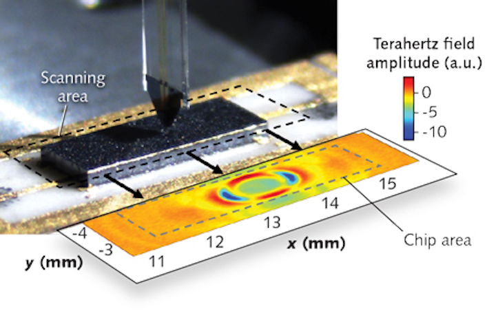
Photonics Applied Terahertz Imaging Terahertz Imaging Tackles Solar Cell And Semiconductor Process Inspection Laser Focus World
Silicon Wafer High Resolution Stock Photography And Images Alamy

Pin On Semiconductor Electronics
Solar Cells And Modules Energypedia Info

12 Epitaxial Silicon Solar Cell Structure The Epitaxial Layer Is Grown Download Scientific Diagram
Why Micron Know How Is Never Executed Transforming Into Yet News Tech Via Www Freebloggerpro Com Memory Chip Computer Processors Bitcoin Mining

Solar Energy Materials And Solar Cells Vol 206 March 2020 Sciencedirect Com By Elsevier

Pin On Damage Mobile Chip Off Data Recovery Allsocket Emmc Emcp Reader

Pdf High Efficiency Silicon Solar Cells

Paytm Launches Credit Card In India In Partnership With Citibank Paypay Me

Learn About What Electrical Impedance Is And How It Combines Both Resistance And Reactance In An Electronic Printable Graph Paper Used Solar Panels Graph Paper
Source : pinterest.com
